- 您现在的位置:买卖IC网 > Sheet目录3873 > PIC16F627-04/P (Microchip Technology)IC MCU FLASH 1KX14 COMP 18DIP
PIC16F62X
DS40300C-page 130
Preliminary
2003 Microchip Technology Inc.
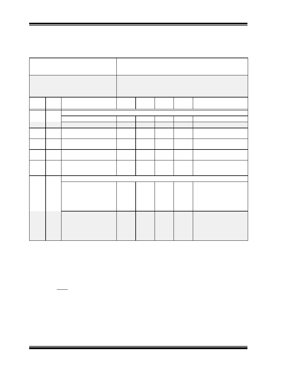
17.1
DC Characteristics: PIC16F62X-04 (Commercial, Industrial, Extended)
PIC16F62X-20 (Commercial, Industrial, Extended)
PIC16LF62X-04 (Commercial, Industrial)
PIC16LF62X-04
(Commercial, Industrial)
Standard Operating Conditions (unless otherwise stated)
Operating temperature
-40
°C ≤ Ta ≤ +85°C for industrial and
0
°C ≤ Ta ≤ +70°C for commercial
PIC16F62X-04
PIC16F62X-20
(Commercial, Industrial, Extended)
Standard Operating Conditions (unless otherwise stated)
Operating temperature
-40
°C ≤ Ta ≤ +85°C for industrial and
0
°C ≤ Ta ≤ +70°C for commercial and
-40
°C ≤ Ta ≤ +125°C for extended
Param
No.
Sym
Characteristic/Device
Min
Typ
Max
Units
Conditions
V
DD
Supply Voltage
D001
PIC16LF62X
2.0
—
5.5
V
D001
PIC16F62X
3.0
—
5.5
V
D002
V
DR
RAM Data Retention
Voltage(1)
—
1.5
—
V
Device in SLEEP mode*
D003
V
POR
V
DD Start Voltage
to ensure Power-on Reset
—V
SS
—
V
See section on Power-on Reset
for details
D004
S
VDD
V
DD Rise Rate
to ensure Power-on Reset
0.05
—
V/ms
See section on Power-on Reset
for details*
D005
V
BOD
Brown-out Detect Voltage
3.65
4.0
—
4.35
4.4
V
BODEN configuration bit is set
BODEN configuration bit is set,
Extended
D010
D013
I
DD
Supply Current(2), (5)
PIC16LF62X
—
0.30
1.10
4.0
3.80
—
20
0.6
2.0
7.0
6.0
2.0
30
mA
A
Fosc = 4.0 MHz, V
DD = 2.0(5)
F
OSC = 4.0 MHz, VDD = 5.5*
Fosc = 20.0 MHz, V
DD = 5.5
Fosc = 20.0 MHz, V
DD = 4.5*
F
OSC = 10.0 MHz, VDD = 3.0(6)
F
OSC = 32 kHz, VDD = 2.0
D010
D013
D014
PIC16F62X
—
0.60
1.10
4.0
3.80
—
20
0.7
2.0
7.0
6.0
2.0
30
mA
A
Fosc = 4.0 MHz, V
DD = 3.0
Fosc = 4.0 MHz, V
DD = 5.5*
F
OSC = 20.0 MHz, VDD = 5.5
F
OSC = 20.0 MHz, VDD = 4.5*
F
OSC = 10.0 MHz, VDD = 3.0*(6)
F
OSC = 32 kHz, VDD = 3.0*
Legend: Rows with standard voltage device data only are shaded for improved readability.
*
These parameters are characterized but not tested.
Data in “Typ” column is at 5.0V, 25
°C, unless otherwise stated. These parameters are for design guidance only and are
not tested.
Note
1: This is the limit to which V
DD can be lowered in SLEEP mode without losing RAM data.
2: The supply current is mainly a function of the operating voltage and frequency. Other factors such as I/O pin loading and
switching rate, oscillator type, internal code execution pattern, and temperature also have an impact on the current con-
sumption.
The test conditions for all I
DD measurements in active Operation mode are:
OSC1 = external square wave, from rail to rail; all I/O pins tri-stated, pulled to V
DD,
MCLR = V
DD; WDT enabled/disabled as specified.
3: The power-down current in SLEEP mode does not depend on the oscillator type. Power-down current is measured with
the part in SLEEP mode, with all I/O pins in hi-impedance state and tied to V
DD or VSS.
4: The
current is the additional current consumed when this peripheral is enabled. This current should be added to the
base I
DD or IPD measurement.
5: For RC osc configuration, current through R
EXT is not included. The current through the resistor can be estimated by the
formula Ir = V
DD/2REXT (mA) with REXT in k
.
6: Commercial temperature only.
发布紧急采购,3分钟左右您将得到回复。
相关PDF资料
PIC18F45J10-I/ML
IC PIC MCU FLASH 16KX16 44QFN
PIC18F24K22-I/ML
IC PIC MCU 16KB FLASH 28QFN
PIC16CR76-I/SS
IC PIC MCU 8KX14 28SSOP
PIC16F887-I/P
IC PIC MCU FLASH 8KX14 40DIP
PIC16CR76-I/SP
IC PIC MCU 8KX14 28DIP
PIC16CR76-I/SO
IC PIC MCU 8KX14 28SOIC
PIC16CR76-I/ML
IC PIC MCU 8KX14 28QFN
PIC16CR74T-I/ML
IC PIC MCU 4KX14 44QFN
相关代理商/技术参数
PIC16F627-04/P
制造商:Microchip Technology Inc 功能描述:IC 8BIT FLASH MCU 16F627 DIP18
PIC16F627-04/SO
功能描述:8位微控制器 -MCU 1.75KB 224 RAM 16I/O 4MHz SOIC18 RoHS:否 制造商:Silicon Labs 核心:8051 处理器系列:C8051F39x 数据总线宽度:8 bit 最大时钟频率:50 MHz 程序存储器大小:16 KB 数据 RAM 大小:1 KB 片上 ADC:Yes 工作电源电压:1.8 V to 3.6 V 工作温度范围:- 40 C to + 105 C 封装 / 箱体:QFN-20 安装风格:SMD/SMT
PIC16F627-04/SO
制造商:Microchip Technology Inc 功能描述:8BIT FLASH MCU SMD 16F627 SOIC18
PIC16F627-04/SO
制造商:Microchip Technology Inc 功能描述:Microcontroller IC Number of I/Os:16
PIC16F627-04/SS
功能描述:8位微控制器 -MCU 1.75KB 224 RAM 16I/O 4MHz SSOP20 RoHS:否 制造商:Silicon Labs 核心:8051 处理器系列:C8051F39x 数据总线宽度:8 bit 最大时钟频率:50 MHz 程序存储器大小:16 KB 数据 RAM 大小:1 KB 片上 ADC:Yes 工作电源电压:1.8 V to 3.6 V 工作温度范围:- 40 C to + 105 C 封装 / 箱体:QFN-20 安装风格:SMD/SMT
PIC16F627-04E/P
功能描述:8位微控制器 -MCU 1.75KB 224 RAM 16I/O RoHS:否 制造商:Silicon Labs 核心:8051 处理器系列:C8051F39x 数据总线宽度:8 bit 最大时钟频率:50 MHz 程序存储器大小:16 KB 数据 RAM 大小:1 KB 片上 ADC:Yes 工作电源电压:1.8 V to 3.6 V 工作温度范围:- 40 C to + 105 C 封装 / 箱体:QFN-20 安装风格:SMD/SMT
PIC16F627-04E/SO
功能描述:8位微控制器 -MCU 1.75KB 224 RAM 16I/O 4MHz Ext Temp SOIC18 RoHS:否 制造商:Silicon Labs 核心:8051 处理器系列:C8051F39x 数据总线宽度:8 bit 最大时钟频率:50 MHz 程序存储器大小:16 KB 数据 RAM 大小:1 KB 片上 ADC:Yes 工作电源电压:1.8 V to 3.6 V 工作温度范围:- 40 C to + 105 C 封装 / 箱体:QFN-20 安装风格:SMD/SMT
PIC16F627-04E/SS
功能描述:8位微控制器 -MCU 1.75KB 224 RAM 16I/O 4MHz Ext Temp SSOP20 RoHS:否 制造商:Silicon Labs 核心:8051 处理器系列:C8051F39x 数据总线宽度:8 bit 最大时钟频率:50 MHz 程序存储器大小:16 KB 数据 RAM 大小:1 KB 片上 ADC:Yes 工作电源电压:1.8 V to 3.6 V 工作温度范围:- 40 C to + 105 C 封装 / 箱体:QFN-20 安装风格:SMD/SMT